Biasing Dynamic Sensors
This guide explains how to control the on-chip parameters (“biases”) of our devices.
What Is A Bias?
Analogue electronic circuits are often parameterised by currents or voltages which are held steady during operation - these currents or voltages are called biases.
These parameters are used to configure sensor sensitivity and response time when generating events.
An introductory paper on the topic is available here.
For even more bias-related information, refer to the Advanced / More Biases-Related Information section.
Understanding The DVS Pixel
A basic understanding of the DVS pixel design is necessary to work effectively with biases; detailed knowledge of analogue electronics is not required. Here is an abstracted diagram of the DVS pixel (taken from Lichtsteiner et al. 2008):
![]()
This shows that there are 3 parts of the DVS pixel:
The first stage is the photoreceptor; there is an amplifier whose job it is to stabilise the voltage across the photodiode and create a voltage signal which is proportional to the log of the light intensity (the “light-related signal”).
The second stage, the “differencing circuit”, rejects the DC component of the light-related signal whenever it is reset, so that the resulting signal doesn’t carry information about the absolute level of illumination.
The third “comparators” stage detects changes in the light-related signal and produces digital events (ON means the light got brighter and OFF means it got dimmer).
Pixel Bandwidth VS Chip Bandwidth
It’s worth disambiguating these terms. The chip bandwidth is the maximum frequency with which events can be transmitted from the chip, if lots are produced by pixels at the same time so that they are queueing inside the chip to be transmitted. For example, this is about 165 M Events Per Second (MEPS) for the DVXplorer and about 12 MEPS for the DAVIS346.
The term “pixel bandwidth” has sometimes been used in different ways in the DVS literature. It might relate to:
The maximum frequency of an oscillating illumination to which the pixel could reliably produce a series of ON and OFF events.
The maximum frequency at which a pixel can produce events in response to fast changes in illumination.
The briefest transient change in illumination that could result in the production of an event.
DVXplorer Biases
On DVXplorer devices (DVXplorer, DVXplorer Lite, DVXplorer Micro), biases are “hidden” and grouped under two simple and explicit parameters to be controlled by the user:
contrastThresholdOn and constrastThresholdOff. Used to control the sensor sensitivity to intensity changes to generate ON and OFF events. The range is from 0 to 17, with the middle value 9 being the default. Smaller values mean a smaller contrast change will be required to generate an event (more events, more sensitivity, more noise), while bigger values do the opposite, requiring a bigger change in contrast before an event is generated (less events, less sensitivity, less noise).ReadoutFPS. Used to control the number of event frames per second in sensor readout (read more in our White Paper). There are many values available, they are named using Readout mode and FPS value:CONSTANT, with this Readout mode, the readout time is guaranteed to be constant (at 1/FPS value) with no data loss. It is only supported as the following values:CONSTANT_100: 10000 µs readout time per frame.CONSTANT_200: 5000 µs readout time per frame.CONSTANT_500: 2000 µs readout time per frame.CONSTANT_1000: 1000 µs readout time per frame.
CONSTANT_LOSSY, with this Readout mode, the readout time is guaranteed to be constant (at 1/FPS value) but it might be smaller than the actual time needed for the full readout (max ~900 µs). There might be some data loss depending on the event load. It is only supported as the following values:CONSTANT_LOSSY_2000: 500 µs readout time per frame.CONSTANT_LOSSY_5000: 200 µs readout time per frame.CONSTANT_LOSSY_10000: 100 µs readout time per frame.
VARIABLE, with this Readout mode, the readout time will try to match the set value (at 1/FPS value) but it may be increased depending on the event load. It is only supported as the following values:VARIABLE_2000: 500 µs minimum readout time per frame.VARIABLE_5000: 200 µs minimum readout time per frame.VARIABLE_10000: 100 µs minimum readout time per frame.VARIABLE_15000: 66 µs minimum readout time per frame.
Davis Biases
On Davis devices (Davis346, Davis346 AER), the different biases are exposed to the user and have varying purposes. This guide will not tell you what exact biases and values to use. It will rather help you to understand the effects of the biases and guide and constrain your search for the optimal biases for your applications.
Understanding And Computing Biases
On Davis devices, biases are currents that are created by a two-stage coarse-fine circuit.
The first stage (the
coarsecurrent value) provides a choice of 8 currents (coarsevalue between0and7) which are logarithmically spaced over more than 6 orders of magnitude, from 25 uA down to 12 pA.The second stage divides the
coarsecurrent value by a digitally programmable value, thefinevalue.Using the
coarseandfinebiases, the maximum value obtainable is that of the coarse bias, whereas the minimum value achievable is zero.
Each Bias is in total composed of 6 values:
Coarse value, as explained aboveFine value, as explained aboveEnabled, whether the bias is enabled or notSex, whether the bias is applied to an N- or P-type transistorType, whether the bias is arranged “normally” or uses a Cascode.Current Level, whether the current level is “normal” or “low”.
The Current Level, Type, Sex and Enabled options are not meant to ever be changed and are not available to
users.
All the previously listed values are stored and set to the device through a single 16-bit integer (one for each bias). Its format is the following:
UCCC FFFF FFFF LCSE

U: Unused

C: Coarse value

F: Fine value

L: Current Level: 1 = Normal; 0 = Low

C: Type: 1 = Normal; 0 = Cascode

S: Sex: 1 = N-type; 0 = P-type

E: Enabled: 1 = Enabled; 0 = Disabled
To compute or convert bias values following the previous scheme, one can use the libcaer functions or the corresponding Excel sheet ( Download).
The interested reader is referred to Delbruck et al. 2010, where the design of the bias generator used on the DAVIS is described in detail.
Important Biases
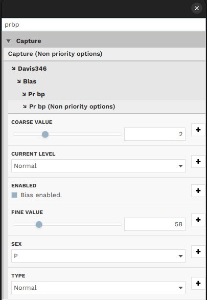
Photoreceptor Bias
Naming: Davis=’PrBp’, DVS=’Pr’
This bias controls the amplifier in the first stage, and limits the speed with which the output of the first stage can respond to changes. An instantaneous change in illumination causes a change in the light-related signal which takes a finite time to readjust. This finite time is highly variable (from microseconds to milliseconds) and it depends on two factors: the level of illumination and this Pr bias. The interaction is as follows. With low illumination and a sufficiently high Pr bias, the adjustment time is dictated by the light level. With high illumination or a low Pr bias, the adjustment time is dictated by the Pr bias. This means that you can use the Pr bias to ensure that this response time is slow, but in order to guarantee a fast response time you need both a high Pr bias and sufficient scene illumination.
Implications for pixel bandwidth and noise: the speed with which a pixel can respond to changes in light (the “bandwidth”) is dictated by several factors; the Pr bias and the scene illumination are two of these factors. If the pixel bandwidth is high then it will detect faster oscillations of illumination; however it will also respond to higher frequency electronic noise, therefore producing more noise events (especially in low lighting conditions).
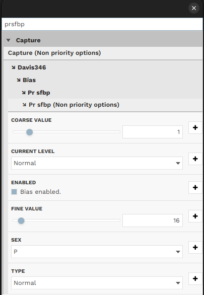
Source Follower
Naming: Davis=’PrSFBp’, DVS=’foll’
Between the first and the second stage, not shown in the above diagram, there is a circuit whose job is to pass the signal from the first stage through to the second stage whilst reducing coupling from the second stage back to the first stage (this is a “source follower”, a type of amplifier). This bias dictates the speed at which this amplifier works. If this bias is set high, it would allow a high pixel bandwidth for fast detection, and at the same time, introduce increased in-band noise, and hence result in increased noise events. However, if this bias is low then it can limit the bandwidth of the pixel in much the same way as the Pr bias can.
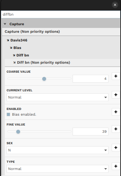
Differential
Naming: Davis=’DiffBn’, DVS=’diff’
This bias controls the amplifier in the second stage. Unlike the Pr bias which has a complex interaction with illumination level, this bias completely determines the speed at which the second stage adjusts to a change in the light-related signal.
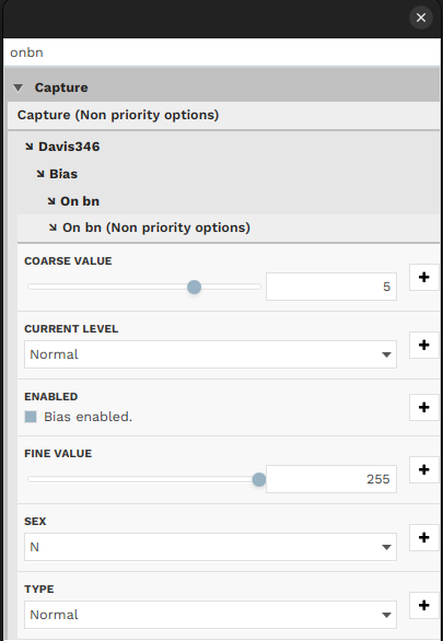
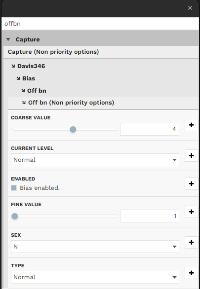
Thresholds For On And Off Events
Naming: Davis=’OnBn/OffBn’, DVS=’diffOn/diffOff’
The size of the change in illumination necessary to produce events is set by varying biases for thresholds. These are independent for increases and decreases in illumination. This is also called setting the “contrast sensitivity” - large thresholds imply a low contrast sensitivity and vice versa.
When the pixel is reset, the output of the second stage to the comparators is a value set by the diff bias. (Here we talk about a “value” for simplicity; the value is a hypothetical current - one which the comparators try to recreate). Once the light-related signal changes, this value changes. If there is more light, the value gets higher and if there is less light then the value gets lower. The change in this value is proportional to the change in illumination, multiplied by the gain of the amplifier. In both DVS128 and DAVIS, the gain is about 20X, so a doubling of the amount of light means a 20-fold increase in this value.
The diffOn bias defines the current level at which the pixel will produce an ON event. This must always be higher than the diff bias, and the ratio between the two defines the change in light level necessary to produce an event. For example, if diffOn is 10 times as big as diff, then a 50% increase in illumination should trigger an event, i.e. ratio / gain = 10 / 20 = 50% relative change expressed as a percentage.
Likewise, the diffOff bias defines the current level at which the pixel will produce an OFF event. This must always be lower than the diff bias, and the percentage change between the two defines the change in light level necessary to produce an event.
Due to mismatch, if you bring either diffOn or diffOff too close to diff then you will see some pixels malfunctioning and at some point the sensor will fail to perform.
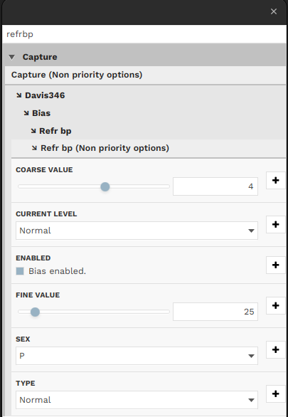
Refractory Period
Naming: Davis=’RefrBp’, DVS=’refr’
When a pixel crosses a threshold it signals to peripheral circuitry in first one dimension then the other. This takes a finite amount of time (typically less than 1 us, although when more than one pixel fires at a time, this time can extend due to queueing). Once the pixel receives the knowledge in both dimensions indicating that communication was successful, it resets itself. This reset requires a finite amount of time (partially dictated by the diff bias).
The refr bias defines the time period during which the pixel will be reset, before it can again start to detect changes in the light-related signal coming from the first stage. Note that this does not stop the first stage from producing the light-related signal - this happens continuously. Thus, any changes that occur during the time it takes for a pixel to first communicate its event and then reset itself are ignored.
We use the term “Refractory period” because of the analogy between a DVS pixel and a nerve cell; in neurobiology this term is commonly used to describe this phenomenon.
How To Change Biases
In DV
For DVXplorer Devices
For Davis Devices
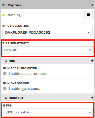
To change a Davis bias in DV, access the camera input module advanced setting, then type the name of the corresponding bias in the search bar.
In dv-processing
All instructions on how to change biases in dv-processing can be found here.
How Are Biases Generated In Our Sensors?
Our dynamic sensors contain digitally programmable bias generators which can produce currents that can vary over many orders of magnitude (from uA down to fA). These currents then produce voltages which can be distributed across a chip to bias many circuits at once, such as pixels.
Having the bias generator on the chip allows us to eliminate the effects of process, voltage and temperature (PVT) variation between chips. Two different instances of one of our sensors will have very similar behaviours if programmed with the same biases, despite significant differences in the fabrication of devices.
The currents produced by the bias generator vary proportionally to absolute temperature - this is a form of temperature dependence which ideally results in constant transconductance operation across temperature, so that the time constants do not vary with temperature.
Our sensors are digitally programmed on startup from the attached USB microcontroller. They can be reprogrammed dynamically in milliseconds in order to alter their behaviour.
For the interested reader, the bias generator circuitry is explained in:
Advanced
More Biases-Related Information
One Event Or Many, In Response To A Change In Light?
If there is a large change in the amount of illumination, will a pixel produce only one event, or will it produce many events in proportion to the size of the change? Depending on the application, one or the other of these behaviours may be preferable. In fact either of these behaviours are possible, and you have some ability to choose between these qualitatively different modes of operation.
We have seen that the speeds of the first and second stage circuits can be modified independently from each other. Consider the example shown in this diagram:
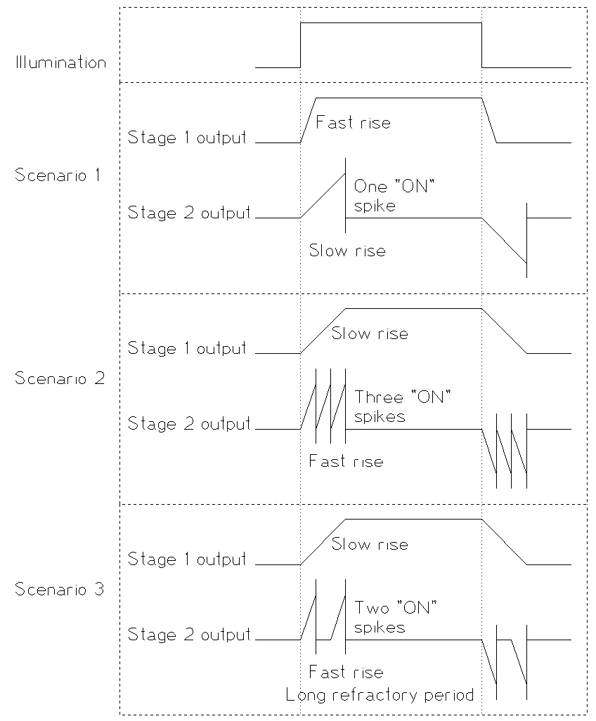
Let’s assume that there is an instantaneous increase in light which is large enough to produce three threshold changes, given the choice of the biases which control the thresholds. There then follows a step back down. This is shown in “Illumination”.
In the first scenario, the DVS is biased with a high Pr and PrSF and a low diff. Stage 1 quickly adapts to the new illumination level. Stage 2 takes longer. By the time it has produced its first spike, the stage 1 output has already settled and there is no more change to detect.
In the second scenario, the DVS is biased with a low Pr and PrSF and a high diff. Stage 1 takes a long time to adapt to the new illumination level. In this time, Stage 2 is able to fire and reset 3 times.
The third scenario is similar to the second, except that the refr bias has been set lower, resulting in a longer refractory period. The stage 2 produces its first event quickly in response to the slow rise of stage 1, but then has to wait until its reset completes. In this time it misses some of the rise of the stage 1 output, so that in the end it only produces two spikes in response to the change.
Remember that the production of lots of events across the chip can cause a delay which may have the same effect as the refractory period in the third scenario. The time to spike, the delay in communication and the refractory period all add up to the period of the pixel, from which the pixel bandwidth is derived.
Sources Of Noise
There are three different reasons why you may see noise in the event stream:
Electronic noise
Background events
APS crosstalk
Electronic Noise
The photodiode and each of the transistors all contribute some electronic noise. In the complete absence of light there is still a small current across the photodiode - this is called the dark current; this current has a certain amount of intrinsic noise. As light level increases, the noise in the photocurrent increases, but it does not do so exponentially, with the effect that there is less noise in the light-related signal, which represents the log of the photocurrent. Thus, especially in low-light conditions, and in darker areas of the scene, the pixels may produce spurious events.
From the second stage onwards there is significant amplification of the signal from the first stage (about a factor of 20), so that any noise introduced to the signal is ignorable compared to the contributions from the devices in the first stage.
The power of the electronic noise is distributed across different frequency bands; if the Pr or PrSf biases are use to limit the bandwidth of the first stage then this reduces the amount of noise that is transduced into spikes (i.e. high-frequency noise is ignored, because the transients are too quick to be detected but rather are smoothed out).
Setting a higher threshold means that only larger deviations in the signal produce events, thus reducing sensitivity to noise at the expense of reducing the contrast sensitivity.
If there is a lot of electronic noise you will see both ON and OFF events coming from pixels. If there is less noise or you have set high thresholds, you may see an occasional ON event from a pixel, quickly followed by an OFF event, or vice versa. This is because the light-related signal is moving around an average value and if there is an occasional large deviation upwards it should be followed by a return towards the average.
Background Events
In well-lit conditions with little electronic noise, there will nevertheless be noise events. These are all of ON type, and from each pixel they arrive with a certain regularity. The rate may be around 1 every 10 seconds or so, depending also on the ON threshold. This is due to a non-ideality in the second stage circuit in which the light-related signal drifts in a given direction in the absence of actual change. The reader seeking a detailed explanation is referred to Lichtsteiner et al. 2008 section III-C. The strength of this drift is also strongly dependent on the amount of illumination - more illumination means more frequent events. The background event rate for pixels directed towards the sun can be 100s of Hz.
There is no way to eliminate these events, although their frequency can be reduced by setting high thresholds. It’s quite common to eliminate both electronic noise and background events in software by applying the BackgroundActivity filter, as described in the jAER code repo.
The drift in the second stage that leads to background events also creates a bias towards ON events. The more infrequently events are produced on average, the more noticeable this bias is. For some applications it may be useful to compensate for this with a higher ON threshold. If event rates are high on average then background events do not occur, because pixels do not have enough time to drift between spikes related to changes in scene illumination.
APS Crosstalk
When a global APS exposure is performed, there can be a burst of excessive events correlated with this. These events have a typically noisy characteristic, although some correlation to expected activity can also be seen, i.e. pixels which were about to spike anyway may be induced to spike by the exposure.
This is caused by an undesirable coupling between certain nodes within the pixel. Reduction or elimination of this may be expected in future designs. Reducing contrast sensitivity can help to reduce this problem.
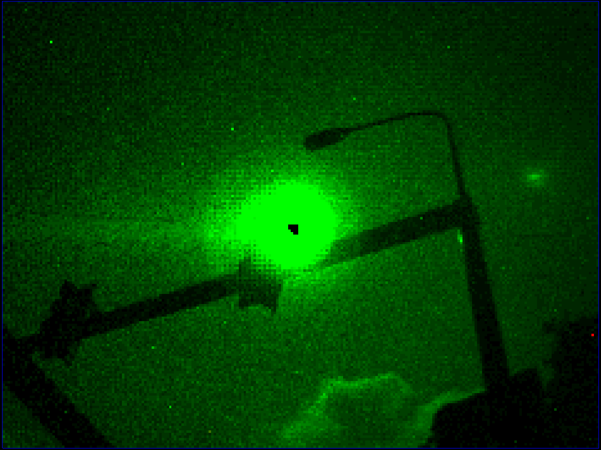
Accumulation Of Noise Can Indicate Light Intensity
Even without APS frames, it’s nevertheless possible to obtain some information about intensity. We have seen that in bright lighting, noise is dominated by regular ON events, which are more frequent from brighter regions. The following image was created by accumulating all the ON events over several seconds whilst observing the sun at a traffic light. The bloom around the sun is apparent:
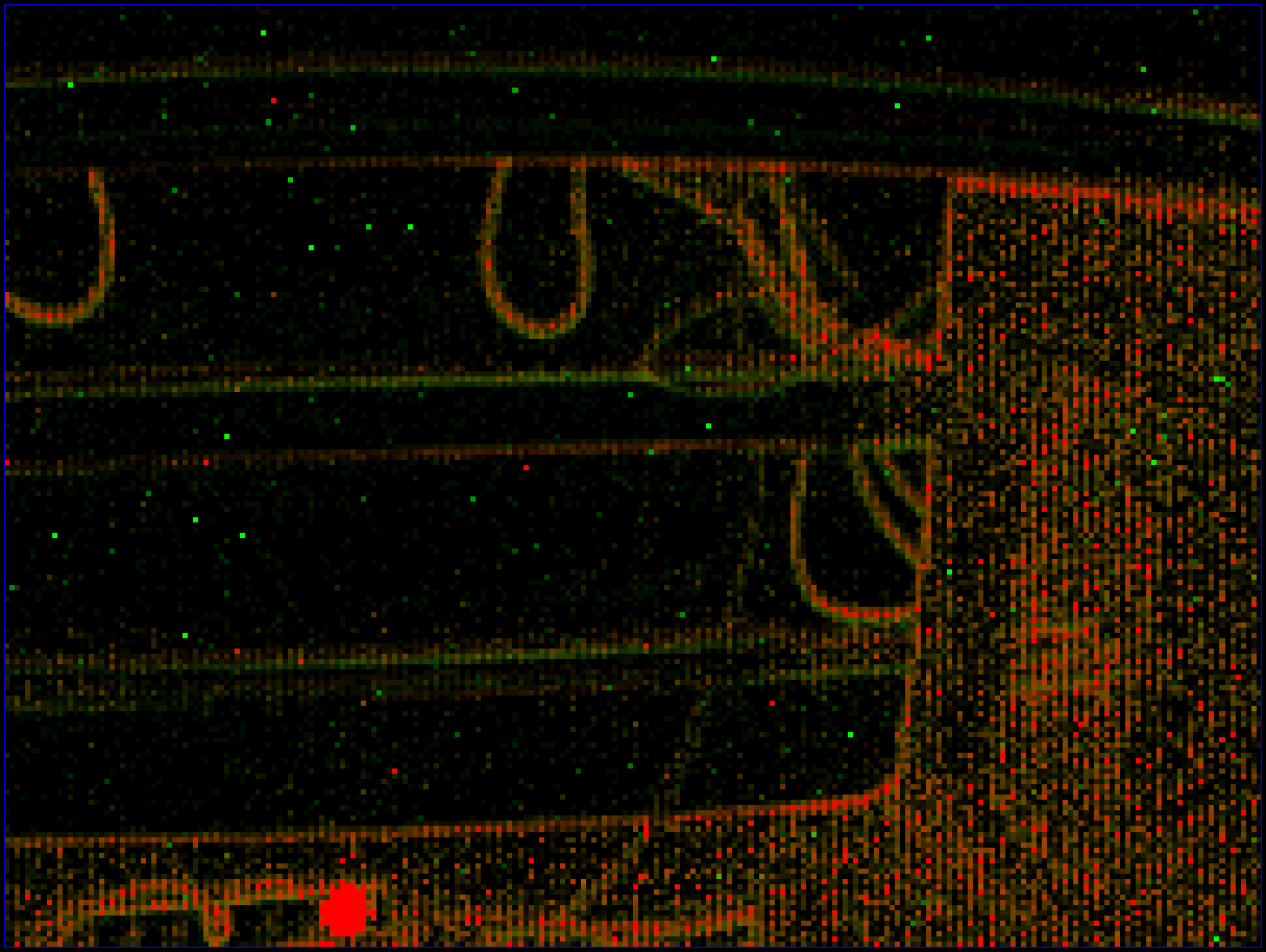
On the other hand, in dark conditions, noise is dominated by irregular ON and OFF events, which are more frequent from darker regions. The following image was created by accumulating all the ON and OFF events over several seconds whilst observing a rats nest of cables under a desk. In this case, the cables are black against a white wall, and produce more events. The additional events from a light to the bottom of the image are due to the light being driven by an oscillating current:
Implications For Power Consumption
The power consumption of the DVS / DAVIS chip is usually dwarfed by the power consumption of the supporting circuitry (CPLD and USB protocol chips) - a typical power consumption for a DVS chip is order 10 mW, whereas the whole device may consume >> 100 mW. However, as embedded applications are explored, the need may arise to limit power consumption of the sensor itself.
Where biases are used in the pixel to create currents, there is one copy of the current for each pixel. Most of these biases do not recreate the same current in the pixel except in specific conditions. For example, the diffOn bias is typically set to quite a high value; however the full current only flows briefly as the pixel approaches the crossing of the ON threshold.
Some currents, however, run continuously. An example is foll / PrSf. If this is set to the maximum value - 25 uA - then across the chip there are 240 * 180 = 43200 copies of a 25 uA current being consumed, i.e. approx 1A, at 1.8V = 1.8W! In some cases it is possible to overload the USB power supply by setting biases inappropriately, leading to the device being rejected by the host computer.
Full characterisation of chip performance vs power consumption is work in progress - we would welcome collaborators in this respect.
Extra Biases On DAVIS Chips
Source code for all Davis parameters
Note: “APS” stands for “Active-Pixel Sensor”. This is the term for standard CMOS image sensors, in which a transistor in the pixel actively transmits a value related to the light intensity read during an exposure. “DAVIS”, in fact stands for “Dynamic and Active-pixel Vision Sensor” - in other words, it is a fusion of DVS and APS circuitry, capable of both producing dynamic events and taking pictures using the same photodiodes. The APS functionality is under control from digital logic external to the chip, including the sequence of exposing and reading out columns and the length of exposures. The following sections only concern the behaviour of the APS functionality that is controlled by the bias generator.
Separation Between APS and DVS
Naming: ‘ApsCasEpc’
This controls a cascode which separates the APS and DVS parts of the pixel circuit, providing a stable voltage to the photoreceptor irrespective of whether an exposure is being performed or not. There are a wide range of values over which this should make no difference to the performance of the sensor.
APS Readout
Naming: ‘ApsROSFBn’
This biases the source follower that performs column-parallel APS readout at the edge of the chip. This needs to be quite high to give short settling times for exposures; providing it is high, the exact value should make little difference to the performance of the sensor.
APS Overflow Level
Naming: ‘apsOverflowLevel’
This sets the lower limit on the range of analogue values that can result from an exposure. However, it has relatively little influence on the range and therefore on the performance of the APS. It does however, need to be quite high to avoid choking the photoreceptor circuit in the case of strong illumination and long exposures.
Differential Cascodes
Naming: ‘DiffCasBnc’
This controls cascodes in the differential comparator stages of the DVS circuit. The purpose of the cascodes is to improve the digital swing of the signals that represent ON and OFF events. This bias should be set higher than diffOn. There is a wide range of values over which this bias will make no difference to performance.
Extra “Overclocking” Biases
The following biases adjust the speed of the digital AER circuitry; you should not normally need to adjust these. Users who need to turn their chip bandwidth up to 11 may experiment with these (the DVS equivalent of overclocking a PC) - we recommend seeking more advice from us in this case.
Passive Load for Digital AER Circuitry
Naming: Davis=’PixInvBn’, DVS=’req’
The actual uses of this bias in the pixel design varies from DVS128 to DAVIS, but the essential role is the same - there are some circuits in the digital AER circuitry of the pixel (passive load inverters) that require a bias for operation. The current dictates the speed at which these circuits work.
Common Resets for Requests
Naming: Davis=’AEPuYBp/AEPuXBp/AEPdBn’, DVS=’PuY/PuX/reqPd’
Individual elements from the arbiters pull up (or down in some cases) on shared request lines which go to the chip-level logic for sending off chip. There is then a chip-level transistor for each of these lines which pulls the line back down in the absence of a pull up, thus resetting the circuit for the next cycle. These biases control the strengths of these various pull-down transistors, and thus have some effect on the speed at which a cycle of AER transmission completes.
Timeout After Row Event
Naming: Davis=’LcolTimeoutBn’ (DAVIS Only)
Pixels may see a change in light and signal their row address, but then the change in light may revert before they have a chance to signal their column address. This leads to a row event which is not followed by any column event (The interested reader is referred to Rapha Berner’s PhD thesis chapter 7). This bias dictates the amount of time between a row event being sent and the X-arbiter giving up waiting for a column request from a pixel. If this bias is too low, row-only events will take a significant amount of time; if this bias is too high, it’s possible that column events might not be sent.
Biases on DVS128
First Stage Amplifier Cascode
Naming: DVS=’cas’
The first stage amplifier contains a cascode transistor whose role is to reduce “Miller capacitance” thus improving the speed and stability of the circuit. There should be a wide range of values over which it makes no difference to the performance, providing that it is significantly higher than the Pr bias.
Injected Ground
Naming: DVS=’injGnd’
This is used for pixel reset to avoid a potential problem (charge pumping leading to spurious resets - the interested reader is directed to Lichtsteiner et al. 2008). The higher this is, the faster a pixel will respond to the acknowledge in order to reset itself. Reducing this bias can cause the chip to output spikes very slowly or stop altogether; above a certain level, this bias will make no difference to performance.